


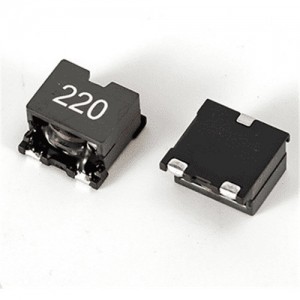
SMD Manufacturer provides straightly unibody large current inductance
Advantages
1) The unique design of our integrated inductor also improves its efficiency. With its low power consumption, it enables electronic systems to operate with minimal energy consumption, thereby extending battery life and reducing electricity costs. This efficiency is critical in today's energy-conscious world as it enables longer-lasting, environmentally friendly equipment.
2)our integrated inductors provide superior performance over a wide frequency range. Whether used in high-frequency applications such as wireless power transmission, or in low-frequency applications such as audio amplifiers, our integrated inductors provide stable and reliable inductance values, ensuring excellent performance and signal integrity.
3) Durability is also a key aspect of our integrated inductors. Our inductors are designed using high-quality materials and manufacturing processes to withstand demanding operating conditions and harsh environments. This durability guarantees a long product life, giving customers peace of mind and confidence in their chosen solution.
4) their technical properties, our integrated inductors are easy to integrate into various electronic systems. Its compatibility with standard manufacturing processes allows seamless integration into a variety of electronic circuits and designs. This ease of integration significantly reduces development time and costs, making it an attractive solution for electronic device manufacturers.
CHARACTERISTICS
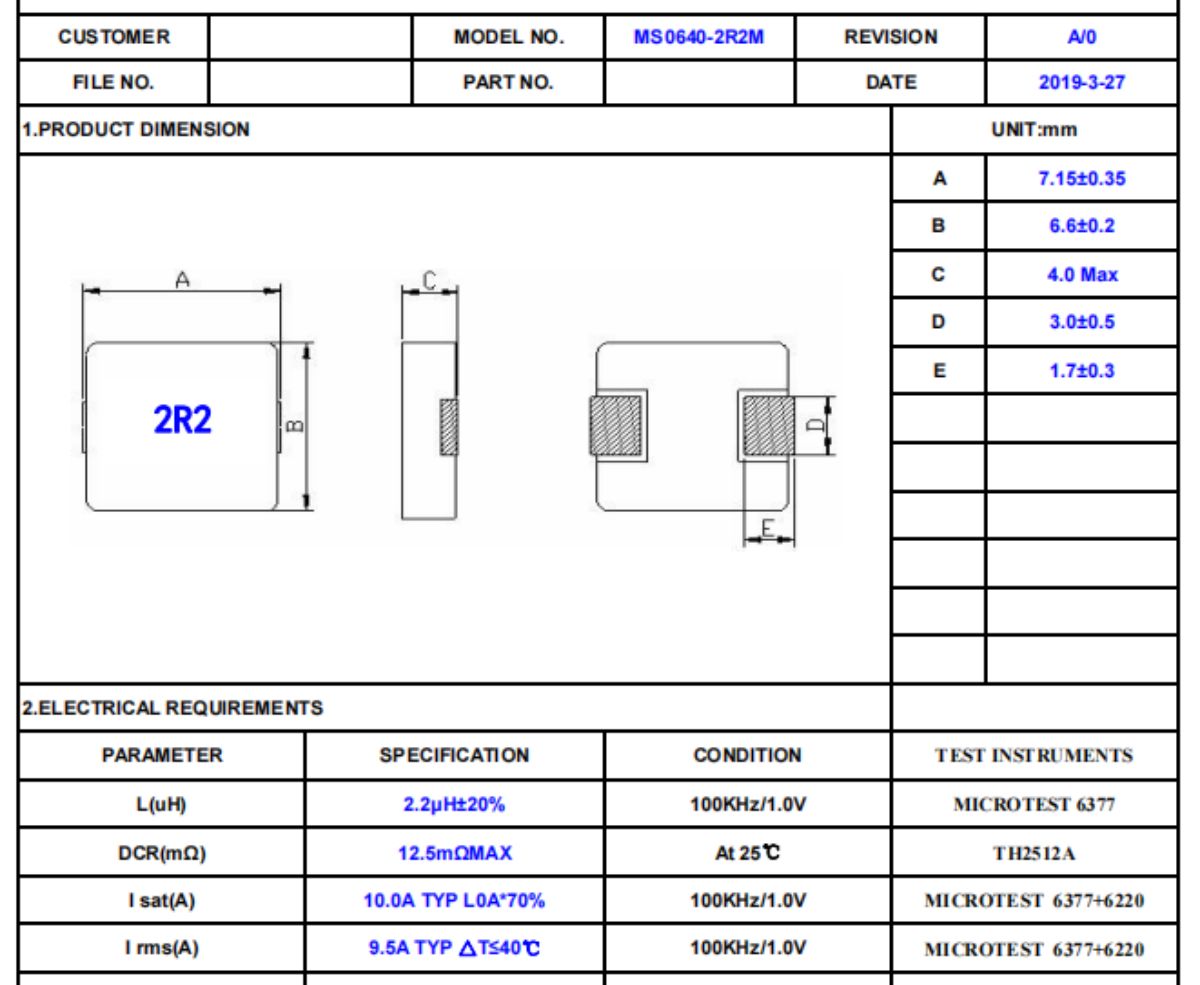
(1). All test data is based on 25℃ ambient.
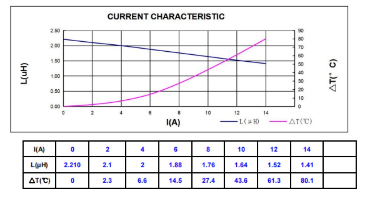
(2). DC current(A)that will cause an approximate △T40℃
(3). DC current(A)that will cause L0 to drop approximately 30%Typ
(4). Operating temperature range: -55℃~+125℃
(5).The part temperature (ambient + temp rise)should not exceed 125℃ under worst case operating
conditions. circuit design, component.PWB trace size and thickness,airflow and other cooling
provision all affect the part temperature. Part temperature should be verified in the den application
(6)special request :(1)Lettering 2R2 on top of the body
specification
Application
(1)Low profile,high current power supplies.
(2)Battery powered devices.
(3)DC/DC converters in distributed power systems.
(5)DC/DC converters for field programmable gate array.
FAQ
Q1. How can we get samples from you ?
A1.If you need a sample test first,Samples are available. Normally we take 2 days to arrange samples. If we have no business record with you before, we need to charge boot samples cost and post courier freight.
Q2. Do you test or check all your goods before delivery?
A2: Yes, we have 100% test and check all goods before delivery.
Q3.How can we get the goods to you?
A3: We can provide our transportation mode resources and price for your reference, and the final transportation mode is up to you under our current conditions
Q4.What is your terms of payment?/When will you send the parts to me?
A4: Full payment. Goods would be shipped in 3-5 work days after payment received, finally depends on quantities.
Q5.How about a refund and replacement?
1. We appreciate your business and offer an instant 7 days return policy. (7 days after receiving the items).
2. If there are any quality problems, please make sure all these items must be returned in their original condition to qualify for a refund or replacement. (Any used or damaged items can not be refunded or replaced)
3. If the items are defective, please notify us within 3 days of delivery.
Products categories
-
SMT/SMD Integrated Inductors Coils & Choke...
-
Power Inductor Flat Wire Coil Magnetically Cros...
-
common mode choke with base toroidal core inductor
-

OEM Inductor Power Choke toroidal PFC inductor
-

Flat Wire Coil Magnetically Crossover Inductor ...
-
Flat Wire Coil Magnetically Crossover Inductor ...